Google and Amazon offer purpose-built AI accelerators for model training and inference alongside general-purpose graphics processing units (GPUs). These custom chips can deliver better efficiency when a workload is stable and large enough to keep the hardware busy, but they exchange some flexibility for that advantage.
The choice is therefore not a simple migration from GPUs to application-specific integrated circuits (ASICs). It is a workload decision shaped by model changes, utilization, software support, development cost and access to manufacturing.
An ASIC narrows the job its hardware must support
An ASIC is designed for a defined application rather than the broad range of software expected to run on a general-purpose processor. It can still contain programmable components, but its data paths, memory movement and arithmetic units are built around a narrower set of operations.
A GPU also contains specialized hardware, including units for matrix and tensor operations, but it preserves a wider programming model. imec IC-Link says GPUs can support training, inference and graphics, while an ASIC removes some general-purpose features to concentrate resources on work such as matrix and tensor math.
Google’s Tensor Processing Unit (TPU) shows how that specialization works. Google Cloud describes a TPU as an ASIC whose matrix-multiply units connect thousands of multiply-accumulators in physical arrays for neural-network calculations. Vector and scalar units handle other operations, so the chip is specialized without being a single fixed circuit for one model.
Stable inference can favor custom silicon
Production inference often repeats the same families of operations under targets for response time, throughput and power use. A custom accelerator can remove hardware that the service does not need and devote more chip area to the operations it runs most often.
That advantage is conditional. imec IC-Link says ASICs can beat GPUs in throughput, latency and energy efficiency when the workload matches the design and a continuous supply of data keeps the chip utilized. A lightly used ASIC or one built for an outdated model can lose the economic benefit even if its peak benchmark is higher.
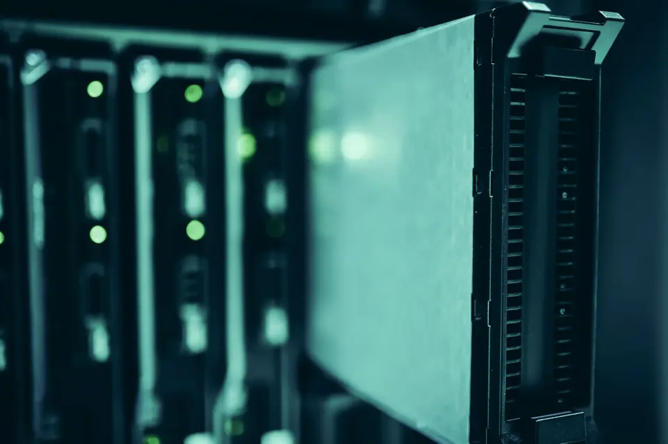
Custom silicon is not limited to inference. Amazon Web Services says its Trainium family is designed for both AI training and inference at scale. Google also makes TPUs available for machine-learning workloads, including distributed training, which means the boundary depends on the chip and software rather than the ASIC label alone.
Development cost changes the calculation
A company can deploy rented or purchased GPUs without funding a new chip design. An ASIC requires architecture work, verification, licensed intellectual property, electronic design automation tools, masks, wafers, packaging and software before volume production begins.
Silicon Analysts estimates that a leading-edge design using a 3- to 5-nanometer process can incur US$30 million to more than US$100 million in nonrecurring engineering costs and require a team of 50 to more than 200 engineers for 24 to 36 months. Its estimate includes US$10 million to US$20 million for a mask set, but those figures are industry modeling rather than a quote from a foundry.
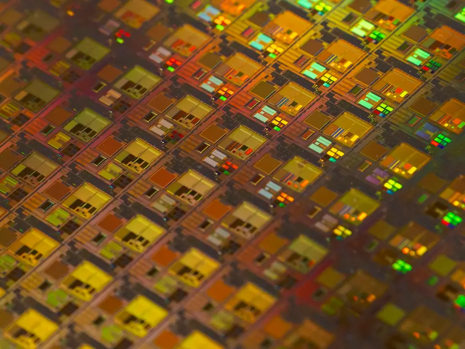
Volume alone does not establish the break-even point. The calculation also depends on the ASIC’s unit cost, the GPU or cloud service it replaces, utilization, electricity, cooling, packaging, software maintenance and the useful life of the design. A model change that requires new hardware can erase projected savings before the first design recovers its upfront cost.
Taiwan supplies design and manufacturing links
Cloud companies do not have to perform every step of a custom-chip program themselves. They can define the workload and architecture while contracting specialists to integrate intellectual property, complete the physical design, arrange fabrication, design the package and manage production.
Taiwan-based Global Unichip Corp. (GUC) documents that role in its own service portfolio. GUC says its services cover specification work, system-on-chip integration, physical implementation, advanced packaging and turnkey manufacturing; it also says Taiwan Semiconductor Manufacturing Co. (TSMC) holds 35 percent of the company and is its sole foundry supplier.
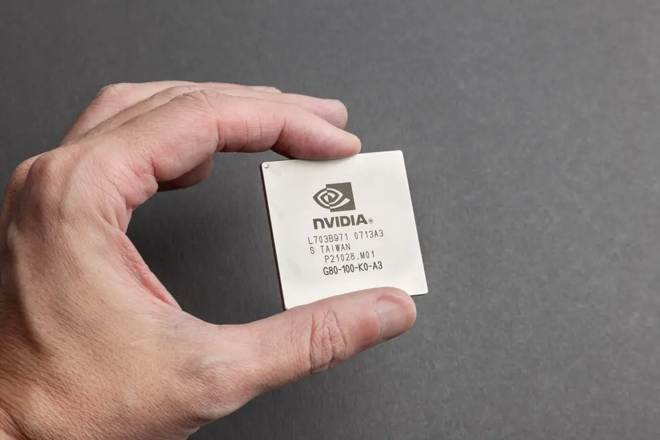
Advanced packaging is part of the accelerator rather than a final protective shell. GUC lists chip-on-wafer-on-substrate (CoWoS), high-bandwidth memory integration and die-to-die interconnects among its capabilities. These technologies connect compute dies and memory, but capacity, yield and package design can still constrain delivery.
GPUs retain an advantage when requirements move
A GPU is usually the lower-risk choice when teams are testing architectures, changing numerical formats or running several unrelated workloads. The same hardware can be reassigned, and mature programming tools reduce the time needed to put a model into production.
Software portability is not automatic on either platform. A framework may support a custom accelerator while particular operators still need tuning, and performance can change with batch size, model shape and compiler version. Buyers need workload-level measurements rather than a comparison of peak specifications.
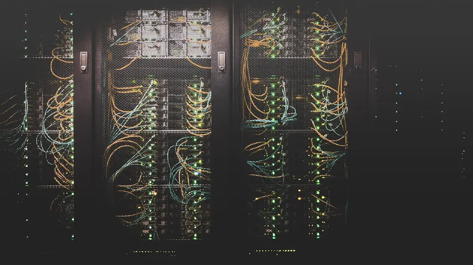
The practical split is a mixed fleet. GPUs can absorb research, changing models and irregular demand, while ASICs can handle selected jobs whose operating profile is predictable enough to justify a specialized design. Training can run on either type, as AWS Trainium and Google TPU demonstrate, so inference is an attractive use case rather than a defining rule.
Frequently asked questions
What is the main difference between an ASIC and a GPU?
An ASIC narrows its hardware around a defined application, while a GPU keeps a broader programmable architecture for different parallel workloads. The narrower design can improve efficiency, but only for work that fits it.
Are ASICs always faster and more energy-efficient?
No. The result depends on whether the workload matches the hardware and whether the system keeps the chip busy. Memory, software and utilization can outweigh a theoretical peak advantage.
Are custom AI chips only for inference?
No. Stable, high-volume inference often suits specialization, but Google TPUs and AWS Trainium also support training. The right division depends on the accelerator generation, model and software stack.
Why would a company still choose GPUs?
GPUs shorten deployment time and can be reassigned when models or workloads change. They also come with mature tools and a larger pool of engineers, while a custom chip commits capital years before its economics are known.
Sources and further reading
- ASIC vs GPU for AI(imec IC-Link)
- TPU architecture(Google Cloud)
- AWS Trainium(Amazon Web Services)
- How Much Does a Tapeout Cost? Fabless Startup Guide(Silicon Analysts)
- About GUC(Global Unichip Corp.)